本文由 简悦 SimpRead 转码, 原文地址 www.righto.com
In 1979, Intel introduced the 8088 microprocessor, a variant of the 16-bit 8086 processor. IBM’s deci……1979 年,英特尔推出了 8088 微处理器,这是 16 位 8086 处理器的变体。IBM 的决定……
In 1979, Intel introduced the 8088 microprocessor, a variant of the 16-bit 8086 processor. IBM’s decision to use the 8088 processor in the IBM PC (1981) was a critical point in computer history, leading to the dominance of the x86 architecture that continues to the present. One way that the 8086 and 8088 increased performance was by prefetching: the processor fetches instructions from memory before they are needed, so the processor can execute them without waiting on the relatively slow memory. I’ve been reverse-engineering the 8088 from die photos and this blog post discusses what I’ve uncovered about the prefetch circuitry.
1979 年,英特尔推出了 8088 微处理器,这是 16 位 8086 处理器的变体。IBM 决定在 IBM PC 中使用 8088 处理器(1981 年)是计算机历史上的一个关键点,导致 x86 架构的主导地位一直持续到现在。8086 和 8088 提高性能的一种方法是预取:处理器在需要指令之前从内存中获取指令,因此处理器可以执行它们,而无需等待相对较慢的内存。我一直在根据芯片照片对 8088 进行逆向工程,这篇博文讨论了我发现的有关预取电路的内容。
The die photo below shows the 8088 microprocessor under a microscope. The metal layer on top of the chip is visible, with the silicon and polysilicon mostly hidden underneath. Around the edges of the die, bond wires connect pads to the chip’s 40 external pins. I’ve labeled the key functional blocks; this article focuses on the prefetch queue components highlighted in red. The components in purple also play a role, and will be discussed below. Architecturally, the chip is partitioned into a Bus Interface Unit (BIU) at the top and an Execution Unit (EU) below. The BIU handles memory accesses, while the Execution Unit (EU) executes instructions. In particular, the BIU fetches instructions, which are transferred from the prefetch queue to the Execution Unit via the queue bus.
下面的芯片照片显示了显微镜下的 8088 微处理器。芯片顶部的金属层是可见的,硅和多晶硅大部分隐藏在下面。在芯片的边缘,键合线将焊盘连接到芯片的 40 个外部引脚。我已经标记了关键功能块;本文重点介绍以红色突出显示的预回迁队列组件。紫色的组件也起着一定的作用,下面将讨论。在架构上,芯片被划分为顶部的总线接口单元(BIU)和下面的执行单元(EU)。BIU 处理内存访问,而执行单元 (EU) 执行指令。特别是,BIU获取指令,这些指令通过队列总线从预取队列传输到执行单元。
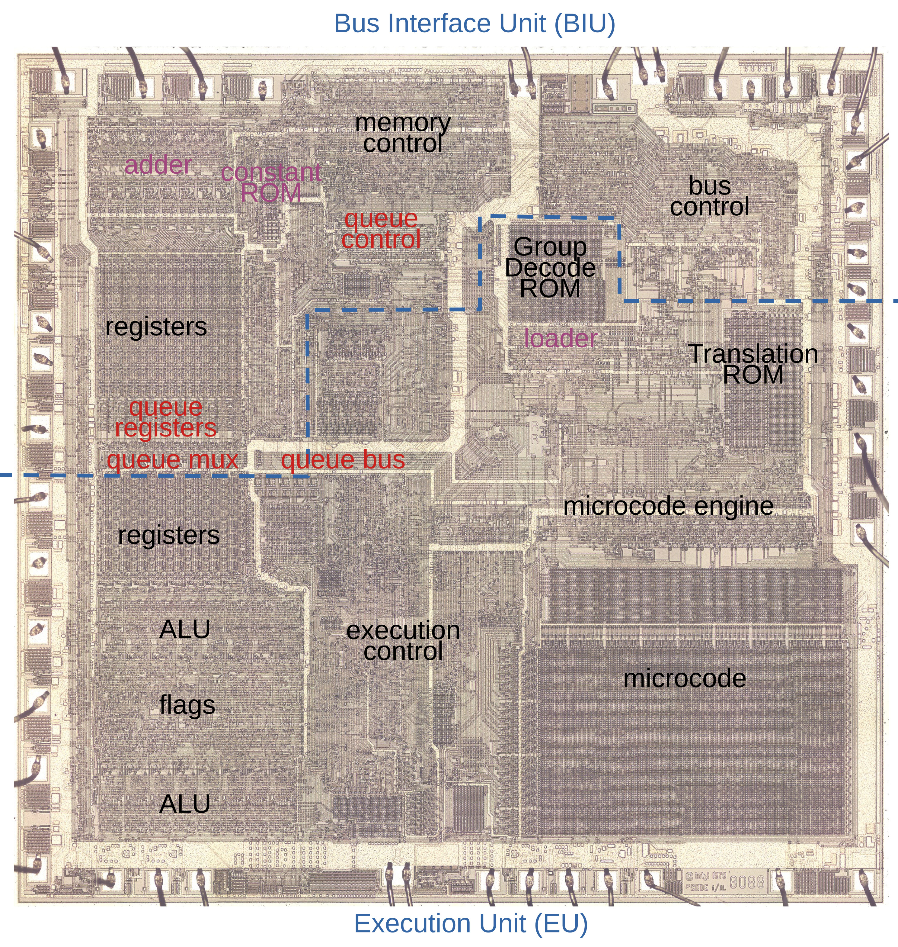
The 8088 die under a microscope, with main functional blocks labeled. This photo shows the chip’s single metal layer; the polysilicon and silicon are underneath. Click on this image (or any other) for a larger version.
8088 模具在显微镜下,主要功能块被标记。这张照片显示了芯片的单个金属层;多晶硅和硅在下面。点击这张图片(或任何其他图片)查看大图。
The 8086 and 8088 processors present the same 16-bit architecture to the programmer. The key difference is that the 8088 has an 8-bit data bus for communication with memory and I/O, rather than the 16-bit bus of the 8086. The 8088’s narrower bus reduced performance, since the processor only transfers one byte at a time rather than two. However, the 8-bit bus enabled cheaper computer hardware. The 8-bit bus was also a better match for hardware based on the older but popular 8-bit Intel 8080 and 8085 processors, allowing the reuse of 8-bit I/O circuitry for instance. Much of the IBM PC was based on the little-known IBM DataMaster, a computer built around the Intel 8085. Thus, selecting the 8088 processor was a natural choice for the IBM PC.
8086 和 8088 处理器为编程器提供相同的 16 位架构。主要区别在于 8088 具有用于与内存和 I/O 通信的 8 位数据总线,而不是 8086 的 16 位总线。8088 较窄的总线降低了性能,因为处理器一次只传输一个字节,而不是两个字节。但是,8 位总线支持更便宜的计算机硬件。8 位总线也更适合基于较旧但流行的 8 位 Intel 8080 和 8085 处理器的硬件,例如允许重用 8 位 I/O 电路。IBM PC 的大部分内容都基于鲜为人知的 IBM DataMaster,这是一款围绕 Intel 8085 构建的计算机。因此,选择 8088 处理器是 IBM PC 的自然选择。
For the most part, the 8086 and 8088 are very similar internally, apart from trivial but numerous layout changes on the die. The biggest differences are in the Bus Interface Unit, the circuitry that communicates with memory and I/O devices, since this circuitry handles 16 bits in the 8086 versus 8 bits in the 8088. There are a few microcode differences between the two chips. One interesting change is that for performance reasons the 8088 has a smaller prefetch queue than the 8086 (four bytes instead of six). (I wrote about the 8086’s prefetch circuity earlier.)
在大多数情况下,8086 和 8088 在内部非常相似,除了芯片上的微不足道但大量的布局变化。最大的区别在于总线接口单元,即与存储器和 I/O 设备通信的电路,因为该电路处理 8086 中的 16 位,而 8088 中的 8 位。两种芯片之间存在一些微码差异。一个有趣的变化是,出于性能原因,8088 的预取队列比 8086 小(4 个字节而不是 6 个字节)。(我之前写过关于 8086 的预取电路的文章。
Prefetching and the architecture of the 8086 and 8088
预取以及 8086 和 8088 的体系结构
The 8086 and 8088 were introduced at an interesting point in microprocessor history, when memory was becoming slower than the CPU. For the first microprocessors, the speed of the CPU and the speed of memory were comparable.2 However, as processors became faster, the speed of memory failed to keep up. The 8086 was probably the first microprocessor to prefetch instructions to improve performance. While modern microprocessors have megabytes of fast cache3 to act as a buffer between the CPU and much slower main memory, the 8088 has just 4 bytes of prefetch queue. However, this was enough to substantially increase performance.
8086 和 8088 是在微处理器历史上一个有趣的时刻推出的,当时内存变得比 CPU 慢。对于第一个微处理器,CPU的速度和内存的速度是可比的。2 然而,随着处理器的速度越来越快,内存的速度却跟不上。8086 可能是第一个预取指令以提高性能的微处理器。虽然现代微处理器具有兆字节的快速缓存 3 作为 CPU 和慢得多的主内存之间的缓冲区,但 8088 只有 4 字节的预取队列。但是,这足以大大提高性能。
Prefetching had a major impact on the design of the 8086 and thus the 8088. Earlier processors such as the 6502, 8080, or Z80 were deterministic: the processor fetched an instruction, executed the instruction, and so forth. Memory accesses corresponded directly to instruction fetching and execution and instructions took a predictable number of clock cycles. This all changed with the introduction of the prefetch queue. Memory operations became unlinked from instruction execution since prefetches happen as needed and when the memory bus is available.
预取对 8086 和 8088 的设计产生了重大影响。早期的处理器(如 6502、8080 或 Z80)是确定性的:处理器获取指令、执行指令等。内存访问直接对应于指令获取和执行,指令需要可预测的时钟周期数。随着预取队列的引入,这一切都发生了变化。内存操作与指令执行没有链接,因为预取会根据需要和内存总线可用时发生。
To handle memory operations and instruction execution independently, the implementors of the 8086 and 8088 divided the processors into two processing units: the Bus Interface Unit (BIU) that handles memory accesses, and the Execution Unit (EU) that executes instructions. The Bus Interface Unit contains the instruction prefetch queue; it supplies instructions to the Execution Unit via the Q (queue) bus. The BIU also contains an adder (Σ) for address calculation, adding the segment register base to an address offset, among other things. The Execution Unit is what comes to mind when you think of a processor: it has most of the registers, the arithmetic/logic unit (ALU), and the microcode that implements instructions. The segment registers (CS, DS, SS, ES) and the Instruction Pointer (IP) are in the Bus Interface Unit since they are directly involved in memory accesses, while the general-purpose registers are in the Execution Unit.
为了独立处理内存操作和指令执行,8086 和 8088 的实现者将处理器分为两个处理单元:处理内存访问的总线接口单元 (BIU) 和执行指令的执行单元 (EU)。总线接口单元包含指令预取队列;它通过 Q(队列)总线向执行单元提供指令。BIU还包含一个用于地址计算的加法器(Σ),将段寄存器基数添加到地址偏移量等。当您想到处理器时,您会想到执行单元:它具有大多数寄存器、算术/逻辑单元 (ALU) 和实现指令的微码。段寄存器(CS、DS、SS、ES)和指令指针(IP)位于总线接口单元中,因为它们直接参与存储器访问,而通用寄存器则位于执行单元中。
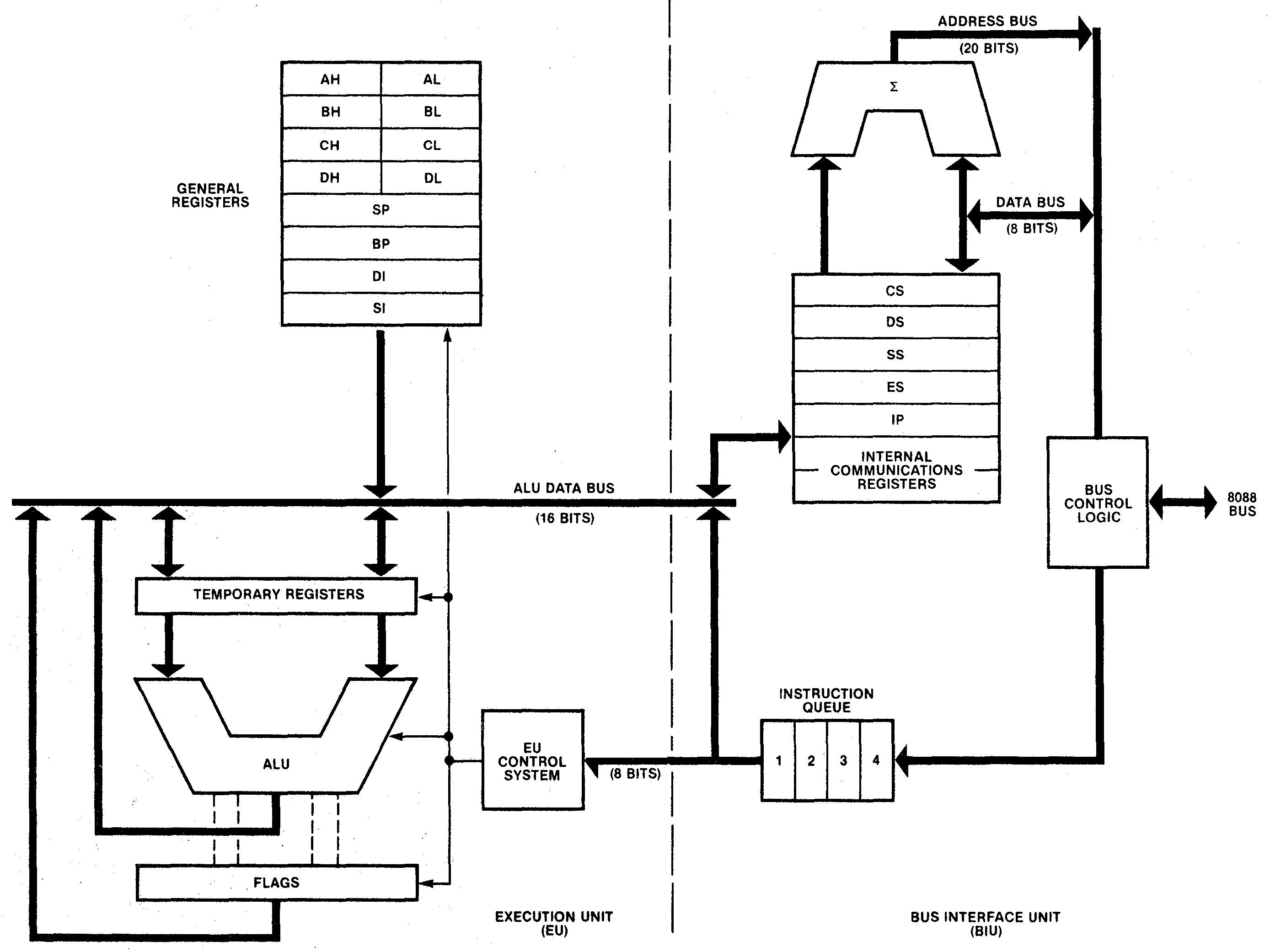
Block diagram of the 8088 processor. This diagram differs from most 8088 block diagrams because it shows the actual physical implementation, rather than the programmer’s view of the processor. The “Internal Communication Registers” consist of the Indirect Register (IND) and the Operand Register (OPR). These hold a memory address and memory data value respectively. From The 8086 Family User’s Manual page 243.
It may seem inefficient for the Bus Interface Unit to have its own adder instead of using the ALU, but there are reasons for the separate adder. First, every memory access uses the adder at least once to add the segment base and offset. The adder is also used to increment the PC or index registers. Since these operations are so frequent, they would create a bottleneck if they used the ALU. Second, since the Execution Unit and the Bus Interface Unit run asynchronously with respect to each other, it would be complicated to share the ALU without conflicts.
Prefetching had another major but little-known effect on the 8086 architecture: the designers were considering making the 8086 a two-chip microprocessor. Prefetching, however, required a one-chip design because the number of control signals required to synchronize prefetching across two chips exceeded the package pins available. This became a compelling argument for the one-chip design that was used for the 8086.4 (The unsuccessful Intel iAPX 432, which was under development at the same time, ended up being a two-chip processor: one to fetch and decode instructions, and one to execute them.)
Implementing the queue
The 8088’s instruction prefetch queue is implemented with four 8-bit queue registers along with two hardware”pointers” into the queue. One two-bit counter keeps track of the current read position from 0 to 3, i.e. the queue register that will provide the next instruction byte. The second counter keeps track of the current write position, i.e. the queue register that will receive the next instruction from memory.5 As bytes are fetched from the queue, the read pointer advances. As bytes are added to the queue, the write pointer advances.
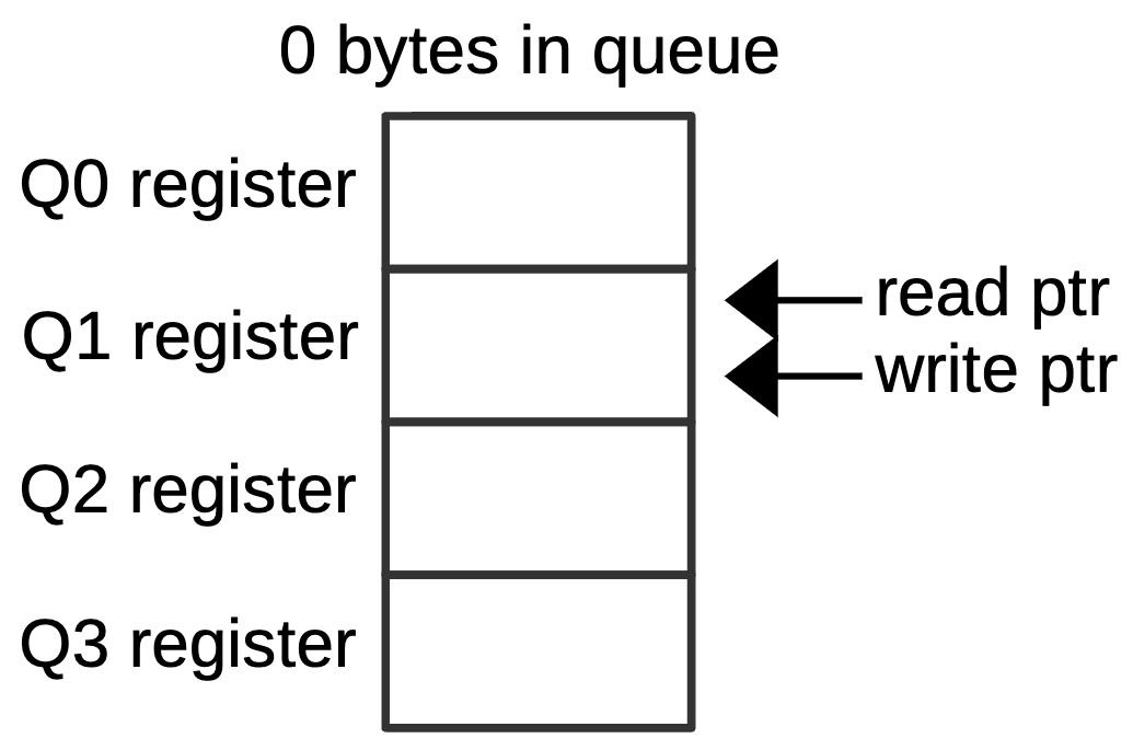
The diagram below shows an example queue configuration with two prefetched bytes. The middle two queue registers (Q1 and Q2) hold data. The read pointer indicates that the Execution Unit will get its next byte from Q1. The write pointer indicates that the next prefetched byte will go into Q3.
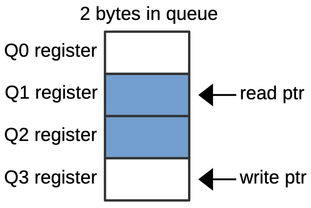
A queue configuration with two bytes in the prefetch queue. Bytes in blue hold prefetched data.
The diagram below shows how the queue pointers can wrap around. In this configuration, two more bytes have been written to the queue (Q3 and Q0), so the queue is full. The write pointer now points to Q1, the same as the read pointer.
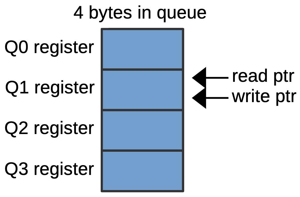
A queue configuration with four bytes in the prefetch queue.
There is an important ambiguity, however. Suppose that four bytes are read from the queue, so the read pointer advances four positions, wrapping around back to Q1. The queue is now empty, as shown below, but the pointers have the same position as the full case above. Thus, if the read pointer and the write pointer both point to the same position, the queue may be empty or full. To distinguish these cases, a flip-flop is set if the queue enters the empty state. This flip-flop generates a signal that Intel called MT (empty).
A queue configuration with the queue empty.
To determine how many bytes are in the queue, the queue circuitry uses a two-bit queue length value, along with the MT flip-flop value to distinguish the empty state. Conceptually, the queue length is generated by subtracting the read position from the write position. However, the implementation does not use a standard subtraction circuit, but instead uses hardcoded logic to determine the two bits of the length, as shown below.
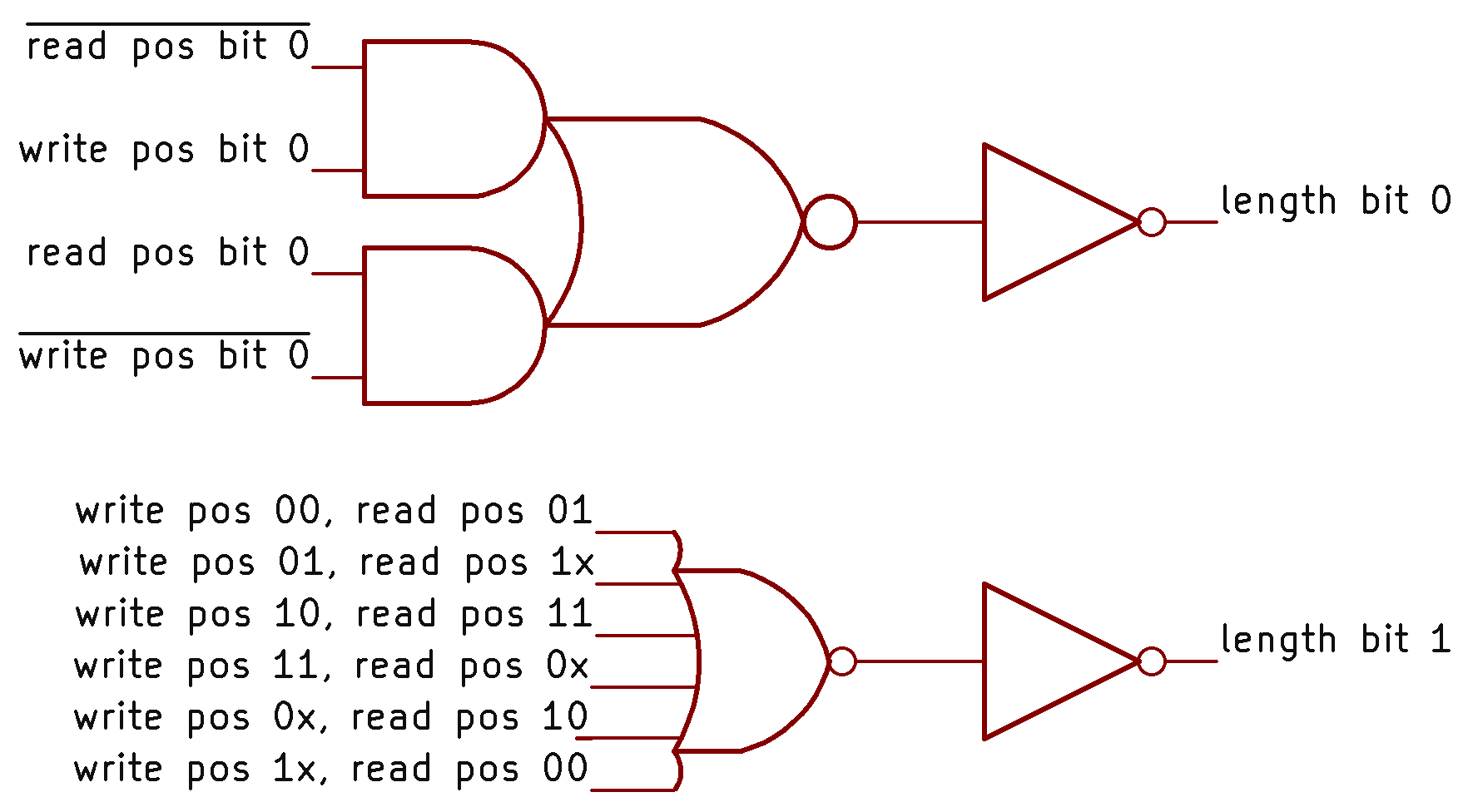
The circuitry to determine the queue length.
The low bit of the length is the XOR of the two positions. In NMOS logic (used by the 8088), an AND-NOR gate is easy to implement, while an XOR gate is difficult. Thus, XOR is implemented as shown in the top circuit. (You can verify that if one input is 1 and the other is 0, the output is 1.) The high-order bit of the length is also based on an AND-NOR gate, one with six inputs. Each input is a combination of read and write positions that yields an output bit 1; each input is computed by a NOR gate, which I haven’t drawn.6 As a result, the amount of logic circuitry to compute the length is fairly large.
The diagram below zooms in on the queue control circuitry on the die, with the main flip-flops and circuitry labeled. The circuitry in the middle computes the queue length with the 6-input NOR gate stretched across the whole region. The flip-flops for the read and write positions are in the lower region. Despite the relative simplicity of the queue circuits, they take up a substantial part of the die. Compared to modern chips, the density of the 8088 is very low; you can almost see the flip-flops with the naked eye. But this isn’t all the circuitry as prefetching also required queue registers and memory cycle control circuitry. Thus, prefetching was a moderately expensive feature for the 8088, as far as die area.
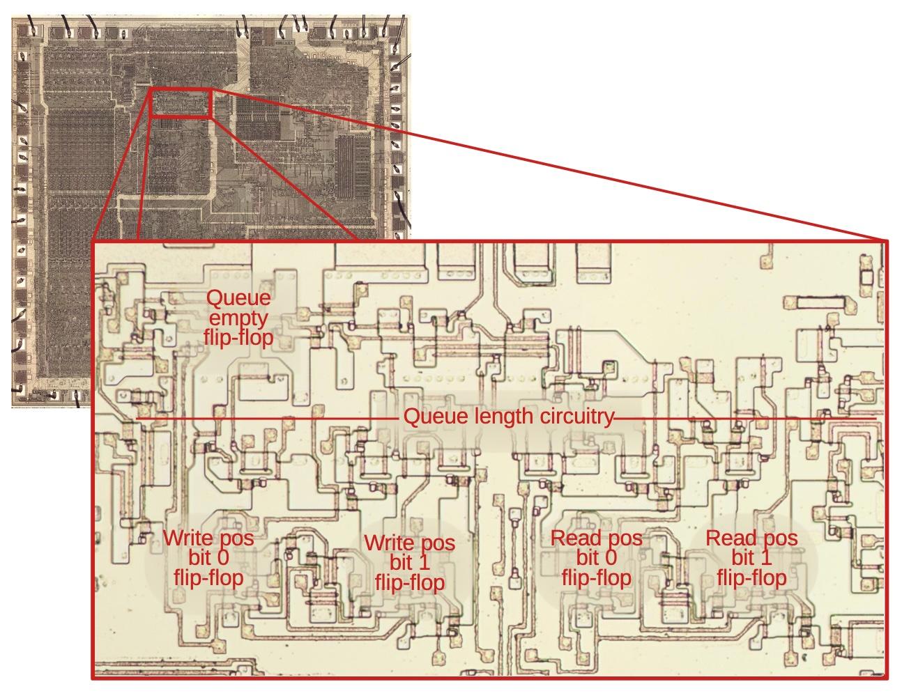
The queue and prefetch circuitry on the die. The metal layer has been removed for the closeup to show the silicon of the underlying transistors.
The loader
The 8086 processor is implemented with microcode: most 8086 machine instructions are broken down into simple micro-instructions that are stored in the microcode ROM. For example, an ADD instruction is implemented through a sequence of micro-instructions to move the arguments to the Arithmetic/Logic Unit, perform the addition, and store the result. The multiple addressing modes are implemented in micro-instruction subroutines that access index registers and compute the memory address. In 1978 the space available for microcode was limited, so the 8086 designers moved a lot of control logic outside the microcode, including insruction fetching and decoding. The relevant part for this discussion is the instruction fetch and decode loop is implemented outside the microcode. A state machine called the “loader” fetches the first one or two bytes of an instruction. A ROM called the Group Decode ROM does a “high-level” classification of the instruction. Simple instructions (such as clearing the carry flag) or prefixes (such as LOCK or selecting a segment register) are performed directly. More complex instructions are dispatched to the microcode engine, which runs the micro-instructions to carry out the instruction.
To decode and execute an instruction, the Execution Unit must get instruction bytes from the Bus Interface Unit, but this is not entirely straightforward. The main problem is that the queue can be empty, in which case instruction decoding must block until a byte is available from the queue. The second problem is that instruction decoding is relatively slow so it is pipelined. For maximum performance, the decoder needs a new byte before the current instruction is finished. A circuit called the “loader” solves these problems by providing synchronization between the prefetch queue and the instruction decoder. The loader uses a small state machine to efficiently fetch bytes from the queue at the right time and to provide timing signals to the decoder and microcode engine.
To explain how instructions are fetched, I’ll first give a brief overview of 8086 instructions. The 8086 instruction format is fairly complicated, with instructions from one to six bytes long. The first byte is the opcode, specifying the instruction. In some cases, this byte completely specifies the instruction, for example PUSH AX to push the AX register to the stack. Most of the instructions, however, have a second byte that specifies the addressing mode and register: the Mod R/M byte. Depending on the addressing mode selected, this may be followed by an 8- or 16-bit memory displacement. Finally, there can be an 8- or 16-bit immediate operand.
In more detail, as the loader requests the first two instruction bytes from the prefetch queue, it generates two timing signals that control the microcode execution. The FC (First Clock) indicates that the first instruction byte is available, while the SC (Second Clock) indicates the second instruction byte. Note that the First Clock and Second Clock are not necessarily consecutive clock cycles because the prefetch queue could be empty or contain just one byte, in which case the First Clock and/or Second Clock would be delayed. The instruction decoding circuitry and the microcode engine are controlled by the First Clock and Second Clock signals, so they remain synchronized with the bytes supplied by the prefetch queue.
At the end of a microcode sequence, the Run Next Instruction (RNI) micro-operation causes the loader to fetch the next machine instruction. However, fetching and decoding the next instruction is a bit slow so microcode execution would be blocked for a cycle. In many cases, this slowdown can be avoided: if the microcode knows that it is one micro-instruction away from finishing, it issues a Next-to-last (NXT) micro-operation so the loader can start loading the next instruction. This achieves a degree of pipelining in most cases; fetching the next instruction is overlapped with finishing the execution of the previous instruction.
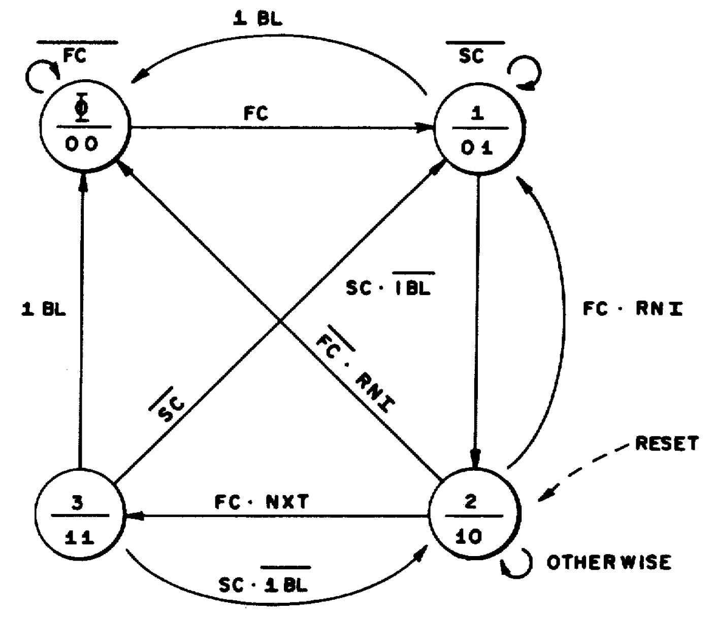
The state machine for the 8086/8088 “loader” circuit. The 1BL signal indicates a 1-byte instruction implemented in logic rather than microcode. From patent US4449184.
The diagram above shows the state machine for the loader. I won’t explain it in detail, but essentially it keeps track of whether it is waiting for a First Clock byte or a Second Clock byte, and if it is performing a fetch in advance (NXT) or at the end of an instruction (RNI). The state machine is implemented with two flip-flops to support its four states.
Microcode and the prefetch queue
The loader takes care of fetching an instruction that consists of an opcode byte and a Mod R/M (addressing mode) byte. However, many instructions have additional bytes or don’t follow this format For example, an opcode such as “ADD AX” can be followed by an 8- or 16-bit immediate value, adding that value to the AX register. Or a “move memory to AX” instruction can be followed by a 16-bit memory address The microcode uses a separate mechanism for fetching these instruction bytes from the queue. Specifically, each micro-instruction contains a source register and a destination register that specify a data move. By specifying “Q” (the queue) as the source, a byte is fetched from the prefetch queue. If the queue is empty, microcode execution blocks until the Bus Interface Unit loads a byte into the prefetch queue. Thus, the complexity of instruction fetching and the prefetch queue is invisible to the microcode.7
A jump, subroutine call, or other control flow change causes the prefetch queue to be flushed since the queue contents are no longer useful. This is accomplished in microcode with the FLUSH micro-instruction, which resets the queue read and write pointers and sets the MT (empty) flip-flop. Note that the queue is flushed even if the target address is in the queue, for example if you jump one byte ahead.
One complication due to the prefetch queue is that the processor’s Instruction Pointer points to the next instruction to be fetched, not the next instruction to be executed. This becomes a problem for a subroutine call, which needs to push the return address. It is also a problem for a relative jump, which is computed from the current instruction. The solution is the CORR micro-instruction, which corrects the Instruction Pointer by subtracting the queue length to determine the current execution position. This is implemented by the Bus Interface Unit, which holds correction constants in the Constant ROM, and subtracts them using the address adder (not the ALU).8
The queue registers
The 8086 and 8088 partition the registers into upper registers (in the Bus Interface Unit) and lower registers (in the Execution Unit). The upper registers are the registers associated with memory accesses (e.g. Instruction Pointer, segment registers) while the lower registers are more general purpose (e.g. AX, BX, SI, SP). The upper registers are connected to two 16-bit internal buses: the B bus and the C bus.
The queue registers are physically part of the upper registers, but are wired into the buses slightly differently, as shown below. In particular, the 8088’s queue registers are written 8 bits at a time from the C bus. (In contrast, the 8086’s queue registers can be written 16 bits at a time to support two-byte prefetches.) When accessing the queue, the queue registers are read 16 bits at a time, but only one byte is transferred to the Q bus for instruction processing.9
The queue registers in the 8088.
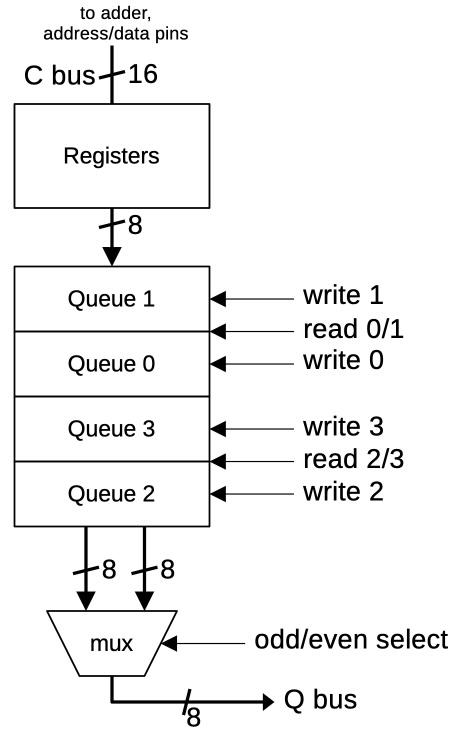
The diagram below shows how the queue registers appear on the die, comparing the six-byte prefetch queue in the 8086 (top) to the four-byte 8088 queue (bottom). The 8086 prefetch registers are structured as three rows of 16-bit registers, while the 8088 prefetch registers are structured as four rows of 8-bit registers. In both cases, each bit is stored in a cross-coupled pair of inverters. The bit lines (not present) are vertical, while the control lines to select a register are horizontal. The layout is different between the processors to support 16-bit versus 8-bit writes. Note the empty space at the bottom of the 8088 registers. Because the rest of the chips are mostly the same, the 8088 couldn’t be”compacted” to avoid this wasted space.
The prefetch registers in the 8086 (top) and 8088 (bottom). For the 8086, the metal and polysilicon layers were removed, exposing the underlying silicon. For the 8088, the polysilicon and silicon are visible.
Intel used simulations to determine the best queue sizes for the 8086 and 8088, balancing the performance cost of prefetching against the benefit. (The cost is that prefetching makes the bus unavailable for other memory or I/O operations.) The prefetch queue is discarded on a jump instruction or other change of control flow, causing the prefetched bytes to be wasted. Thus, as the queue gets longer, the chance of discarding a prefetched byte becomes larger, so the potential benefit of prefetching becomes smaller. Since the 8088 prefetches one byte at a time, compared to two bytes at a time on the 8086, prefetching on the 8088 costs twice as much as on the 8086 in terms of bus cycles used per byte. This changes the tradeoffs in favor of a shorter queue.
Because of the difference in queue lengths, the queue control circuitry is different between the 8086 and 8088. In particular, the 8086 needs three-bit counters for the read and write positions, while the 8088 uses two-bit counters. Because of this, the length computation circuitry is also different between the processors.
I plan to continue reverse-engineering the 8088 die so follow me on Twitter @kenshirriff or RSS for updates. I’ve also started experimenting with Mastodon recently as @oldbytes.space@kenshirriff. If you’re interested in the 8086, I wrote about the 8086 die, its die shrink process and the 8086 registers earlier.
[!NOTE]
转载
本文采用 署名-非商业性使用-相同方式共享 4.0 国际 许可协议,转载请注明出处。


